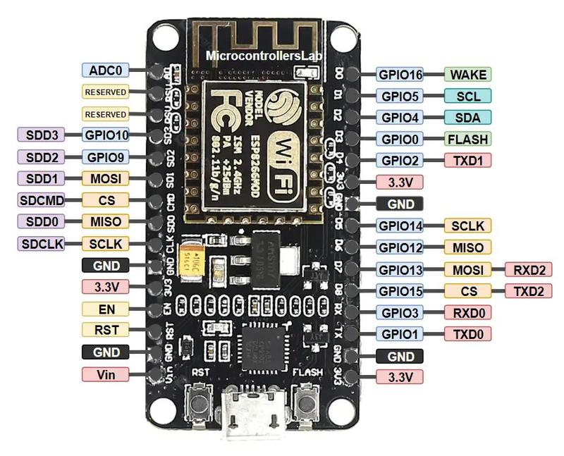
Learning the importance of understanding pins on the ESP8266

While working on my oven thermometer project, I realized that I was going to need more space for more modules and enabling the touchscreen. I also decided to take advantage of the power rails on the side of the breadboards.
I figured out how to use Fritzing, got some custom components for a real representation of my board, and put together the schematic for the single breadboard. After feeling like I had that put together and Fritzing figured out for the most part, I started to plan out my two breadboard configuration.
When I put together the single board, I followed tutorials, but this time I decided to just move it all myself. I also noticed that my pins were a mess. Parts of the temperature sensor were plugged into D0, D1, then D8. The screen was plugged in at seemingly random spots. D3 was unused. I thought it’d be nice if they all were placed sequentially (D0, D1, D2…). I knew what I was doing. I thought…

My first mistake was thinking the ILI9341 only needed to connect to VCC, GND, CS, RESET, OC, and LED. But it turned out that SCK (serial clock) and MOSI (master out slave in) were necessary to get the screen to show more than just the backlight. After riding the struggle bus for a while, I finally went back to a tutorial and fixed the issue. Won’t forget that.
My second mistake was, once again, not fully understanding the pins. Turns out, D3 isn’t just a GPIO pin, but it’s also the “Flash” pin. When I’d go to flash the ESP8266 from my computer with my new configuration (now using D3), my computer couldn’t detect the ESP. It wouldn’t show up in LSUSB at all. I noticed however, that when I took the ESP all the way off the board, I was able to flash it. Now I’ve gotta make sure to always unplug D3 before I go to flash.
I’m currently only using the right side of the ESP. I need to figure out what all the left side is capable of…